1、第一步,打开PCB editor设计软件;

2、第二步,打开菜单栏的 setup-constraints-physical;

3、第五步,点击physical constraits set --all layers,里面有一栏是via设置;

4、第四步,点击默认规则的via,选择一种过孔,也可以点选remove 去除过孔;


5、第五步,设置其他规则的过孔,电源走线的过孔要比其他要大一些;

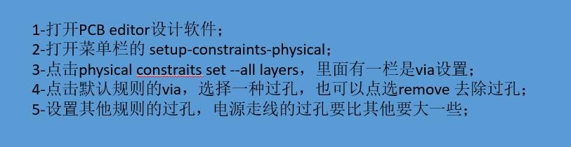
1、1-打开PCB editor设计软件;
2-打开菜单栏的 setup-constraints-physical;
3-点击physical constraits set --all layers,里面有一栏是via设置;
4-点击默认规则的via,选择一种过孔,也可以点选remove 去除过孔;
5-设置其他规则的过孔,电源走线的过孔要比其他要大一些;